Gallium: Cominco has been at the interface between the semiconductor materials and the components industries since the commercialization of the transistor in the early fifties. Based on our commitment to R&D, we have become the largest merchant supplier of several specialty semiconductor substrates including LEC-grown semi-insulating gallium arsenide wafers on this continent.
The following remarks are an attempt to project from this position the potential impact of several advanced uses on the demand for gallium in terms of quantity and quality for the next 10-15 years. This information will be useful in guiding the extractive metallurgical industry in both capital investment and R&D strategy.
Over the past three or four years, it has been practically impossible to escape the hype about the potential of gallium arsenide in our information society, as can be seen in Figure 1.
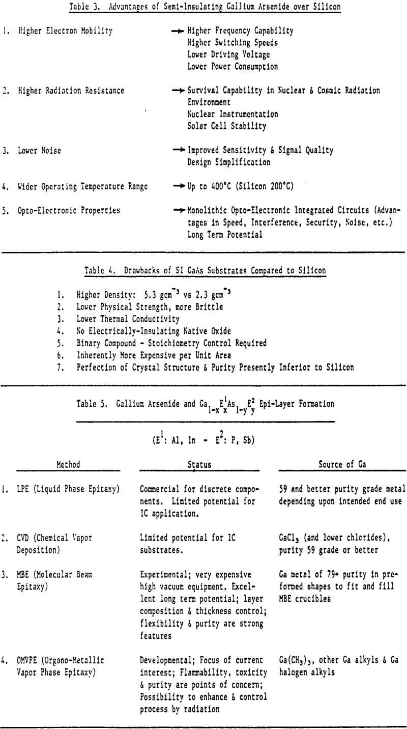
Scientists have recognized long ago that gallium arsenide has several properties which make it a superior semiconductor material compared to silicon. Table 3 shows some of the positive features frequently cited.
Drawbacks of SI GaAs substrates compared to silicon are shown in Table 4. None of these drawbacks, however, present insurmountable obstacles in component production and, consequently, GaAs technology will run its course.
In order to develop the demand picture a brief description is required of how gallium arsenide integrated circuits are being constructed.
The presently prevailing approach is based on the insulating – or at least semi-insulating properties of GaAs; P/N junctions, the key element required for the information society, and conductive channels are created by ion implantation directly into the semi-insulating wafer. This approach is being followed by essentially all presently existing pilot or semi-commercial 1C device lines in North America.
The performance and uniformity of ion-implanted transistors reflects the quality of the substrate in terms of crystalline perfection, stoichiometry and purity. Although useful components can be produced based on presently available substrate material, the industry is pursuing a two-pronged approach to reduce or eliminate shortcomings of the substrate material.
One route pursues systematic improvements in the substrate wafer. Approaches under active consideration are:
- Partial replacement of gallium with indium approximately to the 10 19 atoms cm-³ level. The resulting Ga l-x In x As compound has essentially the same electrical properties as pure GaAs, but the indium atoms apparently lock the lattice with respect to thermal strains resulting in fewer dislocations, however, at the expense of greater brittleness.
- The use of carefully adjusted and controlled thermal gradients during the crystal growing process. Multi-zone heaters, complete immersion in boric oxide encapsulant, and transverse magnetic fields are being tried to reduce dislocations and strain fields.
- The use of starting materials of ever- increasing purity with regard to both metallic and non-metallic impurities.
The second route follows the deposition of an epitaxial layer of adequate thickness on a bulk gallium arsenide single crystal substrate. Hypothetically, there are several reasons to expect improved properties in an epi-layer, depending upon the approach chosen to deposit such a layer.
Table 5 summarizes – approximately in order of increasing significance for IC applications – the key factors in epi-layer production.

Gallium Uses and Consumption
Some of the expected volume applications of GaAs ICs, whether made by direct implant or epi-layer technology, are shown on Table 6.
Another interesting use of gallium in integrated circuit technology is in substrates for magnetic domain memories – frequently called bubble memories. The substrate material in this application is single crystal gallium gadolinium garnet Ga5Gd3O12 grown from the oxide melt by the Czochralski method. A magnetic film is deposited on the garnet wafer and the oriented magnetic domains are formed and manipulated within this structure. Bubble memories captivated the semiconductor industry for several years during the 70s but commercially they have been relegated so far to niche markets by the rapid advancements in silicon memory technology. However, there could be a revival in the future because of the very high density, non-volatile storage capabilities of those memories and their high reliability.
Gallium for Integrated Circuit Applications
Net consumption is defined as that quantity of gallium contained in integrated circuit chips packaged in ceramic or plastic IC packages, tested and shipped to the market plus the losses incurred in recycling scrap materials. As a reference point, in silicon IC processing only 10 to 202 of the electronic grade polysilicon produced ends up In finished functioning devices – 80 to 90% is lost in the form of grinding, sawing, lapping, and polishing sludges, off-spec boule sections, broken wafers, devices not meeting test requirement at various stages, etc. Almost no recycling is taking place because virgin polysilicon is readily available.
In gallium arsenide, because of the greater processing complexity and less mature technology, perhaps only 5 to 152 of the gallium entering into the process will be contained in the functioning chips being shipped. However, because of the rather high intrinsic cost of recovering primary gallium, it is economically attractive to reprocess almost all scrap materials generated during the production of implant, epi- and garnet devices as well as from the production of discrete components (FETs, LEDs) and solar cells. Gallium recycling technology is already relatively well-established with plants operating in North America, Europe, and Japan. We expect that over the long term, at least 90% of the gallium will be recycled from scrap with yields in the order of at least 952 from massive scrap, e.g. crystal ends, broken wafers, etc. and better than 752 from grinding, sawing, lapping and polishing sludges, epi-reactor cleanings, etc.
